Science & techIssue iPhone Duo release date and price: what's new in Apple's first foldable?
Q. What does 2nm mean? 2nm vs 3nm, and is a 2nm chip really 2 nanometers?
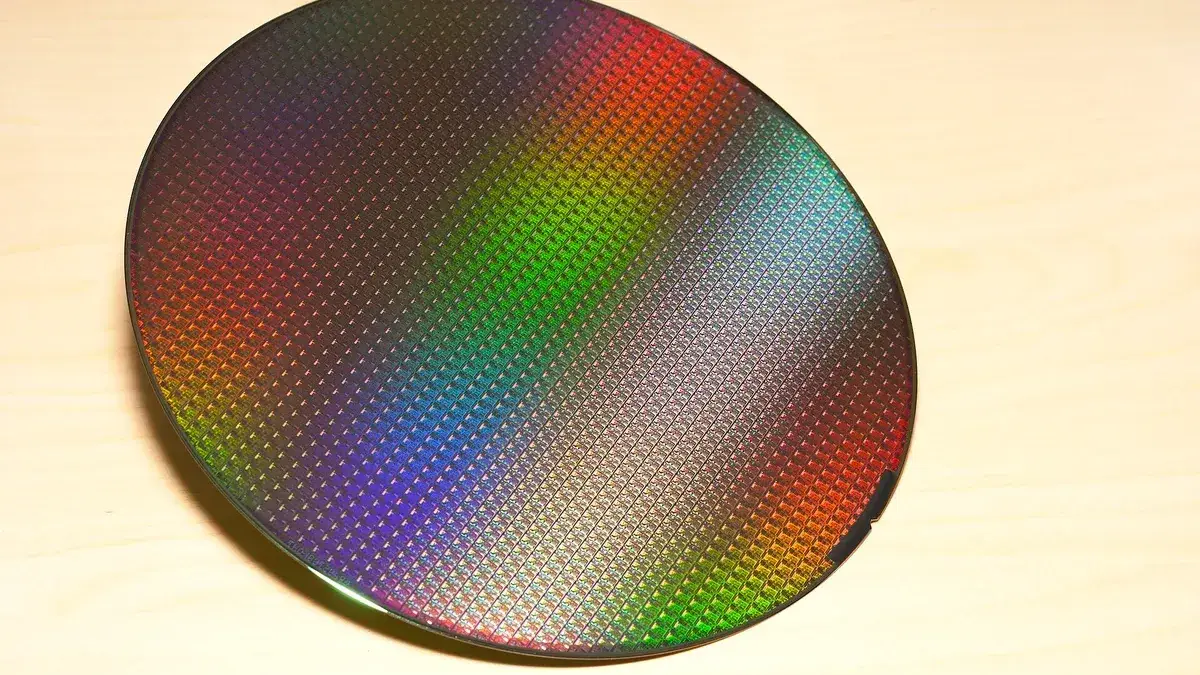
Apple’s iPhone Duo runs on the A20 Pro, a chip Apple says is built on “the latest 2-nanometer process technology.” Two nanometers sounds impossibly small. Is anything inside the chip actually that size? So what exactly does 2nm mean, and how is it different from 3nm?
The short answer: “2nm” is the name of a chipmaking generation, and no key part of a 2nm chip is actually 2 nanometers. The number once matched the real length of a transistor (a tiny electrical switch), but today it works more like a label for “the generation after 3nm.” A 2nm chip packs transistors more densely than a 3nm one, for more speed or lower power.
How small is 2 nanometers?
Nano means one billionth. A nanometer (nm) is a billionth of a meter, so 2nm is two millionths of a millimeter.
According to the US National Nanotechnology Initiative, a human hair is about 80,000 to 100,000 nanometers wide, which makes 2nm roughly 1/40,000 to 1/50,000 of a hair’s width. That is thinner than a strand of human DNA (about 2.5nm), or about six gold atoms side by side, since a gold atom is about a third of a nanometer across. Taken literally, a 2nm process would be carving features finer than DNA.
What is a process node, and what did the number once measure?
A chip is built from an enormous number of transistors. Each has a channel that current flows through and a gate that opens and closes it, and those on and off states are the 1s and 0s of computing. The process is the technology used to manufacture the chip, and a process node is one generation of it.
According to the engineering magazine IEEE (Institute of Electrical and Electronics Engineers) Spectrum, until the mid-1990s a node’s name was simply the gate length of its transistors (how long the gate is over the channel). After that the two drifted apart. On the 130nm node, gates were really 70nm long, and when Intel moved to a new transistor shape called the FinFET at its 22nm node in 2011, the gates measured 26nm, longer than the name itself.
The industry mostly kept the old naming rhythm anyway, and the IEEE’s International Roadmap for Devices and Systems (IRDS) noted in 2023 that chipmakers still have no consensus on node names. One company’s “3nm” need not match another’s.
So is anything in a 2nm chip really 2nm?
Not among the key dimensions. The IRDS 2023 roadmap projects these figures for the “2nm” generation: a gate pitch (the distance from the center of one gate to the next) of 45nm, a tightest metal wiring pitch of 20nm and a gate length of 14nm. Even a single nanosheet, the thin slab that current flows through, is 6nm thick.

The key dimensions of a “2nm” chip are 3 to more than 20 times larger than 2 nanometers. Real chips can differ a little from these roadmap figures.
What is the difference between 2nm and 3nm?
Two things change: transistors are packed more densely, and their shape is different.
Taiwanese chipmaker TSMC (Taiwan Semiconductor Manufacturing Company) said in 2023 that its 2nm process (N2) would offer up to 15% more speed than its enhanced 3nm process (N3E) at the same power, or up to 30% lower power at the same speed, with more than 1.15 times the chip density (how much circuitry fits in a given area). If the names were real lengths, going from 3 to 2 would more than double the density. The actual gain is much smaller.
The shape matters just as much. As transistors shrink, current leaks even when they are off, so chipmakers keep wrapping the gate around more of the channel. Picture stopping a garden hose with your hand. An old planar transistor presses the hose with one finger from above, so water escapes at the sides. A FinFET stands the channel up like a fin so the gate wraps three sides, like a three-finger pinch. A gate-all-around (GAA) transistor stacks thin, flat channels called nanosheets and wraps the gate all the way around them, like a whole fist, which stops leaks best.

In the IRDS roadmap, FinFETs lead through the 3nm class and GAA takes over at 2nm, and TSMC says its 2nm process uses nanosheet transistors. That is not a rule for every chipmaker, though. Samsung announced in June 2022 that it had started initial production on a 3nm process with GAA transistors, calling it the world’s first.
| Feature | 3nm class | 2nm class |
|---|---|---|
| Mainstream transistor | FinFET (Samsung: GAA) | GAA nanosheet |
| Sides the gate covers | 3 (FinFET) | All 4 |
| Gate pitch | 48nm | 45nm |
| Tightest metal pitch | 24nm | 20nm |
| Gate length (high-performance) | 16nm | 14nm |
The pitches and gate lengths are IRDS 2023 projections for its “3nm+” and “2nm” generations.
Is the iPhone Duo’s A20 Pro faster because it is 2nm?
The A20 Pro is the same chip as in the iPhone 18 Pro. Apple says its CPU (central processing unit) is up to 20% faster than the A19 Pro’s, and that, paired with an advanced thermal system that includes a vapor chamber (a thin plate that spreads heat) on the chip, iPhone Duo sustains up to 35% better performance than the iPhone 17 Pro.
Not all of that comes from the process. How fast a phone feels depends on chip design, cooling and software, not just on the process node. Apple also has not said which company makes the A20 Pro, so TSMC’s figures cannot simply be applied to it. Treat “2nm” as a sign of a current-generation chip, and look to real-world reviews for battery life and heat.
In short
A 2nm process is a chipmaking generation, the one after 3nm, and the key features of a 2nm chip are 3 to more than 20 times larger than the name suggests. The real changes are denser circuits and gate-all-around transistors, and the iPhone Duo’s A20 Pro belongs to this generation.
More from this issue
 iPhone Duo release date and price: what's new in Apple's first foldable?
 eSIM vs SIM card: what is an eSIM, and why is iPhone Duo eSIM-only?
 Why do foldable phones have a crease, and does the iPhone Duo have one?
 What does IP68 mean, and can you shower with a waterproof phone?
 What is a vapor chamber, and how does it cool a phone?
People also ask
How small is 2 nanometers?
Two billionths of a meter. A human hair is about 80,000 to 100,000 nanometers wide, so 2nm is roughly 1/40,000 to 1/50,000 of a hair's width, and thinner than a strand of human DNA (about 2.5nm). The key features of a "2nm" chip, though, are 3 to more than 20 times larger than that.
Is a smaller nm number always a better chip?
Within one company, a smaller number usually means a newer, more efficient generation. But chipmakers name their processes in different ways, so the numbers do not compare cleanly from one company to another, and real-world speed also depends on chip design, cooling and software.
What process is the iPhone Duo's chip made on?
iPhone Duo uses the A20 Pro, the same chip as the iPhone 18 Pro. Apple says it is built on the latest 2-nanometer process technology, but it has not said which company manufactures the chip.
Sources
- IEEE Spectrum - A Better Way to Measure Progress in Semiconductors (2020)
- IEEE IRDS - International Roadmap for Devices and Systems 2023 Update: More Moore (PDF)
- TSMC - TSMC Showcases New Technology Developments at 2023 Technology Symposium (26 Apr 2023)
- Samsung Newsroom - Samsung Begins Chip Production Using 3nm Process Technology With GAA Architecture (30 Jun 2022)
- National Nanotechnology Initiative (Nano.gov) - Just How Small Is “Nano”?